
"Nader Engheta superimposed with some of the images related to his research" Credit: Felice Macera.
With the goal of harnessing the untapped potential of Iranian-Americans, and to build the capacity of the Iranian diaspora in effecting positive change in the U.S. and around the world, the West Asia Council has launched a series of interviews that explore the personal and professional backgrounds of prominent Iranian-Americans who have made seminal contributions to their fields of endeavor. Our latest interviewee is Nader Engheta.
Nader Engheta is the H. Nedwill Ramsey Professor at the University of Pennsylvania in Philadelphia, with affiliations in the Departments of Electrical and Systems Engineering, Materials Science and Engineering, Physics and Astronomy, and Bioengineering. His scientific research activities are in nanophotonics, i.e., the study of light-matter interaction at the nanometer scales, enabling manipulation and control of light at the extremely small scales with numerous applications in miniaturization of optical devices and components. He has received numerous international awards for his scientific discoveries and accomplishments. For more details, please check (here)
Tell our readers where you grew up and walk us through your background. How did your family and surroundings influence you in your formative years?
Thanks very much. I am sixty years old and I was born in Tehran in the neighborhood, which used to be called "Chaahaar Raah-e Aziz Khaan" (and later it was called, Khyabaan Hafez (Hafez Avenue)). When I was about 6 years old, my family and I moved to a home in Pasteur Avenue where I started elementary school in Ebn-e-Sina elementary school on Sepah Avenue. I have always been interested in mathematics and physics, particularly with regards to how things work in nature. By 5th grade, I had been ranked No.1 of my class each year prior and one of my teachers suggested that I should "jump" one grade, i.e., move from the 5th grade to the 7th grade. So after I finished my 5th grade exams, I studied 6th grade curricula over the summer and then took the corresponding exams at the end of the summer. I then moved to 7th grade in Hadaf High School No. 1. I spent all of my high school years in Hadaf High School and received my high school diploma in 1973 (1352). I then passed the entrance exam that granted me entrance into university (konkoor saraasary) and entered the Electrical Engineering Department at the School of Engineering (Daneshkadeh Fanni) of the University of Tehran. University of Tehran's Daneshkadeh Fanni has a special place in my heart, and it had a major influence on my love for science and technology. In the summer of 1978, I came to the US to complete higher education at the California Institute of Technology (Caltech) in Pasadena, CA. Caltech is another place that has had a tremendously positive influence on my scientific thinking and instilled in me the love for science and discovery.
What has been your personal key to success? What were the biggest inspirations for your career?
Being passionate about learning new things, and enjoying finding out how the physical laws of nature work are both factors of my personal interest that remain important to me. For example, when I was in high school, one day one of my older brothers, Iradj, was working on a battery-operated transistor radio, and I was puzzled by the fact that sound could come out of this gadget that was not connected to anything. I asked my brother how it worked, and he explained to me that it was the wave coming from the radio station to the radio. This was amazing and magical to me. I became fascinated with waves and followed his suggestion to study electrical science and engineering to discover more about how waves work. That is why I decided to go to the EE department in Daneshkadeh-e-Fanni.
Your current research activities include an impressive list of nanophotonics, metamaterials, plasmonics, nano-scale optics, graphene optics, imaging and sensing inspired by eyes of certain animal species, optical nanoengineering, time-reversal symmetry breaking and nonreciprocity, microwave and optical antennas, mathematics of fractional operators, and physics and engineering of fields and waves. Can you share the highlights of the momentous amount work you have achieved?
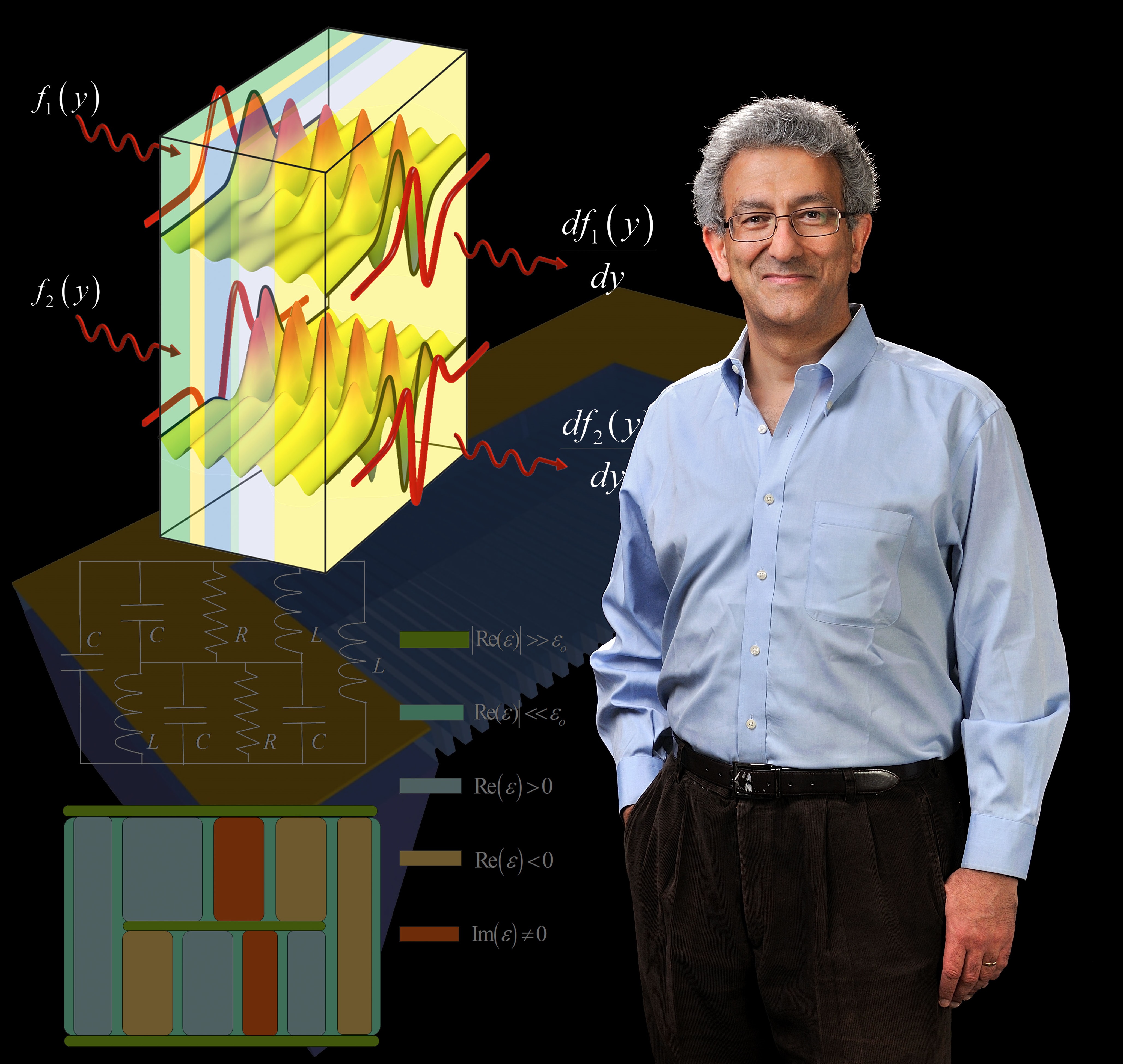
I am very interested in the physics and engineering of fields and waves, and this includes how optical waves and electromagnetic waves interact with structures. This interaction can happen on many different scales, e.g., on the macroscopic scale, the microscopic scale, and the nanometer scales. Just to give you a feel for this dimension and size, imagine you get a single strand of your hair, which has the diameter of about 0.1 of a millimeter (which is about 100 microns). Now imagine you divide this thickness by a factor of 1000, you get to a size that is about 100 nanometers. That is the size that is comparable with the wavelength of visible light (which ranges from 400 to 700 nanometers). At this small dimension, materials can behave differently in their interaction with light. For example, take a block of gold, which is usually yellowish. Now, if you get a nanometer-scale particle of gold with the size around 100 nanometers, and you illuminate it with light under the microscope, you may see different color (e.g., red or green, etc.). So, the same gold may behave differently at the nanoscale. In my group we are interested in exploring how light interacts with the structure at these scales, and how we can utilize it to have nanostructures with unconventional features and useful functionalities, as I explain later here.
We are also exploring how it would be possible to have one-atom-thick optical devices, such as one-atom-thick fibers, which could be much, much thinner than the current optical fibers in the market. These would be thinnest possible waveguides.
Another area of interest lies in how the eyes of some of animal species "see" the world around them. Some of the species such as ants and bees can see some characteristics of light, such as polarization, that the human eyes cannot see. Inspired by the eyes of such species, we have made camera systems that can image the world around us in a very different way. I elaborate more on this below.
In your group, you focus on the areas of metamaterials and plasmonic optics to see how the concept of metamaterial can be used to bring the fields of electronics, photonics, and magnetics together and also how they can be used to generate some interesting ideas for future devices.. Can you first tell our readers what metamaterial is and then about wave interaction with metamaterials? How can you use it for future devices?
The field of metamaterials is indeed about constructing structures that exhibit unusual characteristics in their interaction with waves. Ordinary, naturally available materials, such as water, air, metal, are made of atoms and molecules in special arrangements that determine how light interacts with them. However, in metamaterials, which are typically made of small blocks of materials (such as blocks of metal) as "inclusions" embedded in host media, we consider other level of arrangements, which can be engineered such that when the light illuminates them, the entire bulk of this structure may behave in a way that is very different from how each individual block and the host behaves. The prefix "meta" means "beyond" in Greek, so the term metamaterials refers to structures that go "beyond" the ordinary materials. For example, can we make a structured material that when it is put around an object, it can cause the incoming wave to go around the object (instead of being "splashed" away from the object), and thus the object can become essentially "invisible"? This is an example of topics that the field of metamaterial explores and in my group we have worked on this subject. Another topic for which we have utilized the concept of metamaterials is in bringing the field of electronics and photonics together. As you know, the field of electronics has seen amazing developments in the 20th and 21st centuries, and it continues to evolve. One of the reasons for the great success of electronics is that there exist "modularized" circuit elements, such as capacitors, inductors, resistors, transistors, diodes, etc. The field of optics did not have such modularized elements before. In my group we decided to change that, and by utilizing the concept of metamaterials, we developed the new circuit paradigms, which I named "optical metatronics". In these optical metatronics, properly designed nanoparticles and nanostructures, when illuminated by light, function as "modularized" optical circuit nanoelements, such as optical nanocapacitors, optical nanoinductors, and optical nanoresistors. Through these developments, we have shown that by arranging these nanoparticles next to each other we can construct circuits that work with light (instead of electric currents), and therefore they are much smaller, much faster, and have many more capacities. We envision that in the future such optical nanocircuits can be one million times smaller than the conventional current-day circuits.
You are a leading figure in the nascent field known as metamaterials. Combining several branches of physics and engineering with a healthy dose of nanotechnology, the discipline is focused on creating human-made features that can bend and manipulate waves in ways that nothing in nature can. You could potentially develop "cloaking devices," which can bend waves around an object, rendering it effectively invisible. Can you elaborate on this?
Yes, I spoke briefly about this above. Here is how it works: The way we "see" an object is by sensing the waves that have been splashed away from the object. However, properly designed metamaterials can manipulate the waves that hit the object, and therefore can cause the wave to go around the object, instead of being splashed by the object. Consequently, the wave is splashed less, and therefore the object may become less "visible".
Could you share with us your exploration on optical domains or imaging?
In our work in biologically-inspired imaging and sensing, we have been inspired by the functioning of the eyes of some animal species, such as bees and ants. Light has several characteristics, such as its wavelength, intensity, and polarization, to name a few. Human eyes can pick up only two of these three characteristics, i.e., its wavelength and intensity, which then encode them as color and brightness. However, our eyes cannot effectively "see" the third feature of light, i.e. its polarization. But there are animal species, such as some invertebrates, that have eyes with this capability. They use this ability to see better in their environments, and they can utilize it in navigation. In my group, we were inspired by these interesting features in nature, and have developed imaging and sensing systems that can also capture this feature of light. With such cameras, we can see things in the world that our eyes could not ordinarily see.
Could you share with us some of your ongoing work in your areas of interest, present some of the opportunities and challenges in these areas, and forecast some future directions and possibilities?
In my group, we are currently working on a variety of research programs involving the interaction of light with nanoscale matters and nanomaterials. One of these projects directly deals with how we can utilize materials in a manner such that as the light goes through them the light is able to "do mathematics". In other words, we are exploring how we can use materials to do mathematical computation with light, i.e., we are investigating how "materials can become computing machines at the nanometer scale", how "materials can solve equations", and how we can do "mathematics with light", kind of like "photonic calculus". In the development of the field of optical metatronics, we have already shown that "materials can become optical circuits", and now we are very interested to take this optical metatronics to the next stage and see if we can do more complex things, such as "solving equations with materials". Another research program in my group focuses on how we can design materials that have unusual and "extreme" values for their parameters such as near-zero refractive index. Such values lead to fascinating properties in wave physics, field engineering, and particularly quantum optics (i.e., how photons interact with atoms as the atomic levels). We also continue our work on biologically-inspired sensing and imaging for a variety of different applications.
How different is the education system in the United States from that of Iran? You regularly participate in many conferences and give seminars. Have you done a similar program in Iran?
I have had very positive experiences with both systems. In Iran--at the time I was a student--we learned a lot about mathematics, engineering, and science, but less about the connections between these fields. In the US, you are encouraged to go after the boundaries among these fields and explore new paradigms that can benefit from those domains. For example, our work on biologically-inspired imaging is an example of such an interdisciplinary area. It began by bringing the biology and optics of eyes into the technology of imaging and sensing, and as a result new discoveries occurred in this interdisciplinary topic.